Sony Introduces Multi-Layer SPAD Depth Sensor for Automotive LiDAR Applications, an Industry First Contributing to Future Mobile Security with Improved Detection and Recognition for Automotive LiDAR Applications Sony Semiconductor Solutions Corporation Sony Semiconductor Corporation Announces Upcoming Multilayer Sensor Depths SPAD IMX459 for automotive LiDAR applications directly using TimeofFlight (dToF).
IMX459 SPAD Depth Sensor
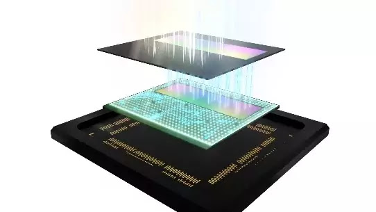 |
| SPAD ToF depth sensor stacked configuration (Top: SPAD |
methodology, an industry first. This product combines a 10μm small square pixel single-photon avalanche diode (SPAD) and distance measurement processing circuitry in a single die to provide a 1 / 2.9 form factor that provides accurate and fast measurement at a simple distance. As a multi-layer SPAD depth sensor for automotive LiDAR. As announced on September 6, 2021. Pixel structure that uses avalanche multiplication to amplify the electrons of an incident photon, causing an avalanche cascade.
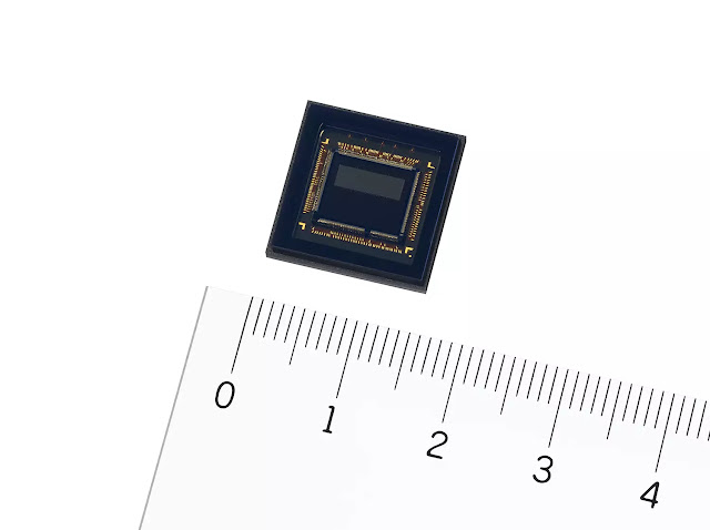 |
| IMX459 SPAD ToF depth sensor for automotive LiDAR applications |
Based on the method for determining the effective pixels of the image sensor. Meanwhile, technical obstacles remain to the growth and market entry of LiDAR, including the need to further improve distance measurement performance, provide greater safety and reliability regardless of environment and conditions of use, and a solid-state design to achieve greater compactness. and lower cost. A number of initiatives are being implemented to address these challenges. Among the various methods used to measure LiDAR distances, the SPAD pixel is used as a type of detector in the dToF sensor.
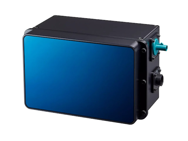 |
| Mechanical scanning LiDAR reference design |
which measures the distance to an object by determining the time of flight (time difference). Time) of light emitted by the source until it returns to the sensor after being reflected from the object. Using Sony technologies such as backlit pixel structures, composite profiles and CuCu interconnects created during the development of the CMOS image sensor, Sony has achieved a device architecture. The unique chip incorporates SPAD pixels and distance measurement processing circuitry on a single die. This design helps to achieve a small pixel size per 10 µm square, providing a compact shape and high resolution of approximately 100,000 effective pixels in a 1 / 2.9 type format.
 |
| Imaging example (point cloud) |
It also provides more efficient photon detection and increased sensitivity, delivering fast and accurate distance measurements with 15 cm range resolution, from long to short. Semiconductor technology is used in electronic components and devices without moving mechanical parts. Uninterruptible power supply technology through copper elements connected by superimposing pixel part (upper chip) and logic circuit (lower chip). With silicon through-wiring (TSV), where the connection is achieved using electrodes inserted around the perimeter of the pixel area, this approach provides more design freedom, improved performance, and improved performance. …
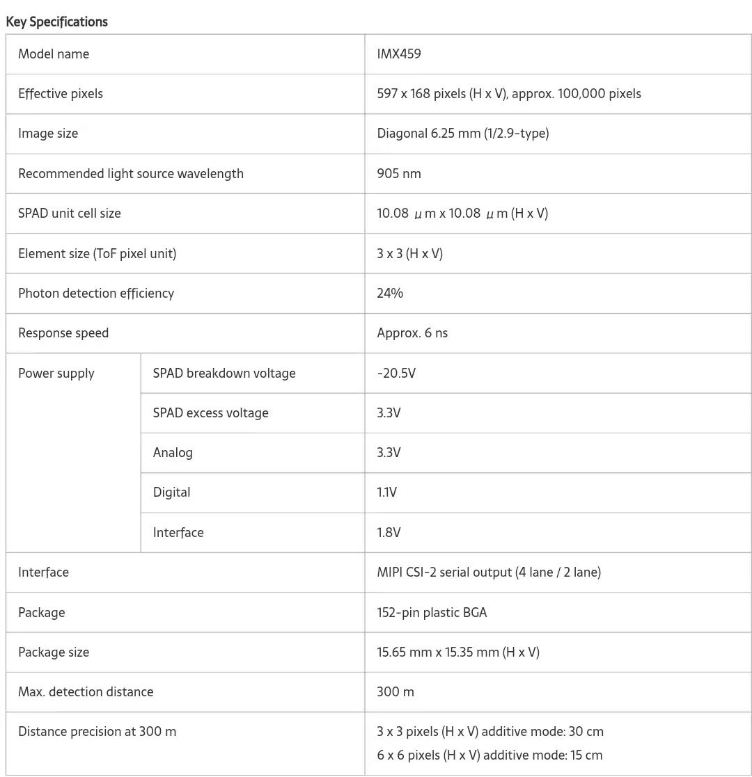 |
| Sony IMX459 Specifications |
High speed and high precision distance measurement thanks to multi-layer configuration with 10 μm square SPAD pixels and rangefinder and logic chip equipped with rangefinder (below). This makes it possible to realize a configuration with a circuit located at the bottom of the pixel chip while maintaining a high aperture ratio resulting in a small square pixel with a size of 10 µm. It also uses the plane of the incident light with irregularities on its surface to refract the incident light, thereby improving the absorption rate.
These characteristics result in a high photon detection efficiency of 24% at the 905 nm wavelength commonly used in automotive LiDAR laser light sources. It is possible to detect distant objects with low reflectivity at high resolution and resolution at long distances. In addition, an active charging circuit is included in the circuit section, which comes with a per-pixel CuCu connection, which provides a response speed of approximately 6 nanoseconds during normal photon operation.

