Four high-performance, low-power chips have won the Carbon Trust label for measuring product carbon emissions, paving the way for reducing carbon emissions.
Samsung’s Green Manufacturing Efforts Continue to Expand Product Range Samsung Electronics, a global leader in advanced semiconductor technology, announced today that four LSI products have received the Carbon Trust Product Carbon Footprint Label, the first Samsung logic chip to do so. With the Semiconductor Industry’s first carbon certification for memory chips from the Carbon Trust in 2019, Samsung has expanded its ESG (Environment, Social and Governance) spectrum by globally recognizing its green logic chip.
Samsung also achieved the Carbon Trust’s first three industry standards for carbon, water and waste in June 2021. World advises companies on their capabilities in a sustainable manner. The Carbon Trust also measures and certifies the environmental impact of organizations, supply chains and products. Among the various certification categories of the Carbon Trust, Samsung Systems LSI products have received a CO2 label.
The carbon footprint of a chip informs consumers about the environmental impact of a product and its manufacturing process. Obtaining a CO2 measurement label is an important first step in reducing carbon emissions, as it verifies current carbon emissions against globally recognized specifications (PAS 2050), which Samsung can use as a benchmark to measure future carbon savings.“We are delighted that our efforts to protect the environment have received worldwide recognition,” said Songai Chan, senior vice president and director of DS Sustainability Management at Samsung Electronics.“We will continue to meet our carbon reduction targets and expand our efforts to a wider range.
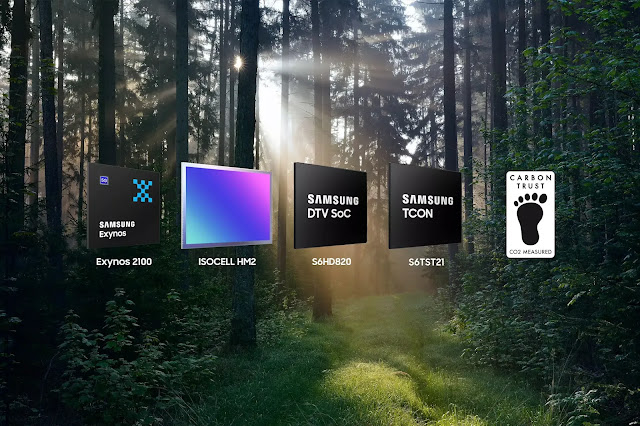
Exynos 2100
Exynos 2100 Based on the 5nm EUV process technology, the Exynos 2100 is an integrated leading mobile processor. Samsung’s first 5G chipset for high-end mobile devices. performance up to 26 billion operations per second (TOPS) with more than twice the energy efficiency of the previous generation
ISOCELL HM2
ISOCELL HM2 ISOCELL HM2 is a 0.7 µm image sensor that has pioneered the ultra-high definition market. also has faster autofocus, 9-pixel combining and 3x lossless zoom.
DTV SoC
DTV SoC (S6HD820) Samsung’s DTV SoC (S6HD820) is an important component of television as the picture quality changes from 4K to 8K. NPU (Neural Processing Unit) DTV SoC enables artificial intelligence technology to improve picture quality and sound processing.
TCON(S6TST21)
TCON takes video data from the DTV SoC and converts it according to DDI (Display Driver IC) requirements. TCON baud rate is important when transferring high definition video data in DDI quickly. (S6TST21) combines two 8K chips at 60Hz (Hz) to minimize power loss.


