SRAM memory scaling is no longer possible. It’s a reality that will have an impact on the whole sector. This is a major issue for NVIDIA, Intel, Apple, AMD, and almost every other chipmaker and startup. The good news is that this issue might be resolved by a new memory technology. It can get computers closer to a significant speed increase and cost decrease. Allow me to clarify.
We require additional memory
Every year since the invention of transistors in 1947, we have managed to reduce their size. We accomplished a terrific job with this: the transistors were first measured in centimeters, and thereafter in micrometers. We can now produce chips in large quantities at 3 and 4 nm. For instance, the most recent Apple M4 chip is in N3, and Qualcomm’s Snapdragon X Elite chip is in the N4 process node. Memory also long followed this same trend, growing in tandem with circuit logic. However, the fact that it is now over presents a serious issue for the whole sector.
SRAM has been the preferred memory for all applications requiring speed and quick access times for the previous 60 years. SRAM is made up of latches, which are often constructed using four to six transistors. SRAM memory is highly favored due to its superior performance and low power consumption, particularly during idle periods. It is the best memory available, and the logic of the cores is intimately integrated with it. We can access the data in the 250–500 picosecond range since it stores data near the cores and we continue to use GHz rate clocks.
The overall pattern indicates that memory capacity per chip is continuously rising. A closer look at the latest chips produced by companies like Apple, AMD, NVIDIA, and Intel reveals that they are all increasing the amount of memory on their chips. For instance, NVIDIA is increasing the amount of cache that is included in each of their new GPUs. Similarly, with every successive iteration of its M processor, Apple is allocating an increasing amount of space to larger caches. The issue is that cache memory uses up an increasing amount of the chip because it doesn’t scale as well as logic.
Scaling issue
Let’s attempt to ascertain what is wrong in this situation. SRAM is manufactured in the same process node as the chip logic and is integrated into the semiconductor die, unlike all other forms of memory. Since chip logic has mostly followed Moore’s law, we can get roughly twice as many transistors in every manufacturing node at the same price. Memory cells, regrettably, do not scale at the same pace. Memory scaled with a factor of 1.8 at first, then 1.4, and this value decreased with each additional process node.
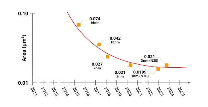
By the time TSMC unveiled its most recent N3 technology, it was obvious that SRAM scaling was finished. In reality, the N3 node provided a transistor scaling factor of x1.7 and SRAM scaling of x1.0. The bit cell size at the next upgraded N3B process node is only 5% smaller than at the N5 node, as you can see from the following chart, which shows that it has an area of 0.021 µm². This isn’t only TSMC’s difficulty; the industry as a whole is affected, including the Samsung and Intel fabrication facilities.
Why is scaling so ineffective? These memory cells are unique, to put it simply. The SRAM cell itself is made of transistors, but it has a different structure. Due to its extreme sensitivity, it is very susceptible to changes in the manufacturing process, such as alterations in the dopant or transistor threshold voltage. It seems that the continued scaling of smaller memory cells is hampered by differences in the production process. As we switch from FinFET to GAA technology and replace fins with nanosheets, which presents additional technical problems, the issue might not get better and might even get worse.
As a result, SRAM will inevitably take up more chip surfaces with every additional production node, increasing costs. The main problem here is that SRAM is required to complete the task. A processor core’s performance will be slower if there is insufficient SRAM since data must be retrieved from a greater distance, using more power.
Chiplets
Upon realizing that scaling SRAM would be impossible, we turned to chiplets as a backup plan. merely placing RAM directly over the CPUs. When AMD initially unveiled its V-cache technology in 2022, it was a big deal because it let us have a lot more cache memory. Here, AMD deserves a great deal of praise for its forward-thinking ideas. Naturally, TSMC deserves some of the credit as well, since AMD made use of TSCM’s 3D SoIC (“System on Integrated Chips”) packaging technology. The 64MB of extra L3 cache that was essentially layered on top of the CPU die greatly improved the speed of numerous apps, including gaming.
Generally speaking, this concept of piling objects vertically on top of one another is quite clever. The ability to combine and match chipsets in various process nodes is one of its greatest benefits. For instance, you could construct a chip with the most sophisticated process node for the logic and then add any memory die, say in an older process node, on top of the stack. In this instance, we can make use of the increased density and speed of the core’s logic to employ a larger SRAM on top, or we can use an older SRAM die that is more affordable, dependable, and has a higher yield.
Innovative Memory Technology
Chiplets don’t solve the problem; they might help with costs and possibly even memory. This is the reason the industry has been searching for a substitute memory technology for a long time. Thus, several novel memory technologies are being developed, such as phase-change memory, resistive memory, ferroelectric memory, and magnetic RAM. It’s interesting to note that every memory technology type has advantages and disadvantages. Certain types are better suited for certain areas, while others are more suited for power or speed. Some types also have higher bandwidth and faster access times than others. Furthermore, we are aware that every CPU and GPU has a variety of memory types, each with its specifications. Their methods for storing data differ significantly in their speed.
With access times in the millisecond range, SRAM is the fastest. and low power is required. Tens of nanoseconds is the access time for DRAM, which is slower and relies on a single transistor and capacitor. The slowest of all is flash memory. The next step is to differentiate between memory types that are volatile and non-volatile. Because SRAM and DRAM are volatile, data is only stored there while power is available.
Thus, it is evident that latency, size, and power consumption are the most important factors in SRAM memory. Therefore, using chalcogenide alloy in a superlattice structure, Stanford researchers have created a novel PCM material dubbed GST467, which was just reported in Nature. It functions essentially as a memory cell made of glass placed between two electrodes, which changes between its crystalline and amorphous phases in response to a high current pulse. In this video, I go into further information about it.
because it fulfills every requirement we have, this new technology has a ton of promise. Its access time is quick—nanoseconds or less. Because it operates at a low voltage, contemporary logic processors may use it. The study claims that it is denser than SRAM from TSMC in the 3N process node, for example, and has the smallest dimensions to date (0.016 um^2). It is around 23% more efficient in terms of area. That is incredible!
Naturally, this is very fresh research, and before it can be widely used in commerce, there are still a lot of technological obstacles to overcome. Integrating it with the present CMOS production flow, lowering the programming current, enhancing reliability, etc., is one of the problems.
Future Opportunities
There is a tendency toward packing more and more memory into chips, a trend that is becoming increasingly important as artificial intelligence (AI)-based applications gain traction. For the L1 and L2 cache, I think latch-based SRAM technology will remain the same for the foreseeable future—at least a few decades. Thus, we will witness it consuming an increasing amount of space and money. After that, as soon as new memory technologies reach fast enough access times—within the region of a few nanoseconds—we will see them initially appear in DRAM and maybe expand to L3 cache.


