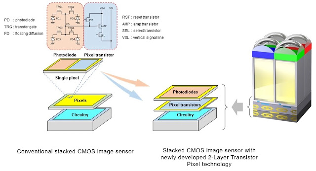
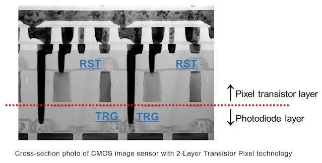
Sony’s semiconductor business announced earlier today that it has developed the world’s first stacked CMOS image sensor with two layers of pixels. transistors in pixels This unique design doubles the sensor’s light-gathering capability when compared to a traditional stacked CMOS sensor. More room is beneficial to both photodiodes and transistors.
Now, what does that really mean in terms of image quality? By increasing the sensor’s saturation level, Sony has also expanded the chip’s dynamic range or the span from the darkest to brightest values it can detect. It has also lowered output noise levels by increasing the amplifier transistors.
It’s vital to remember that just because the signal saturation level has been doubled doesn’t mean the dynamic range has been doubled as well. (It also doesn’t indicate a 50% reduction in noise levels.) Other aspects of the sensor’s architecture will also play a role, and Sony has yet to quantify the DR or noise reduction improvements it has made.
First, look for technology in smartphones and small-pitch sensors.
Nonetheless, it’s evident that a significant move forward in both areas is possible. We anticipate that this revelation will have the biggest impact on smaller, higher-resolution sensors like those used in smartphones, before spreading to bigger sensors, as it did when backside-illuminated sensor designs initially became popular.
Because each photodiode has less surface area, to begin with, the potential for improvement in a tiny, high-resolution sensor is larger than it would be in a sensor with low resolution and/or a big surface area. Sony acknowledges this, stating that their technology would enable “the realisation of progressively high-quality photography such as smartphone images.”


