Samsung working a new Under Display camera For Z Fold 5
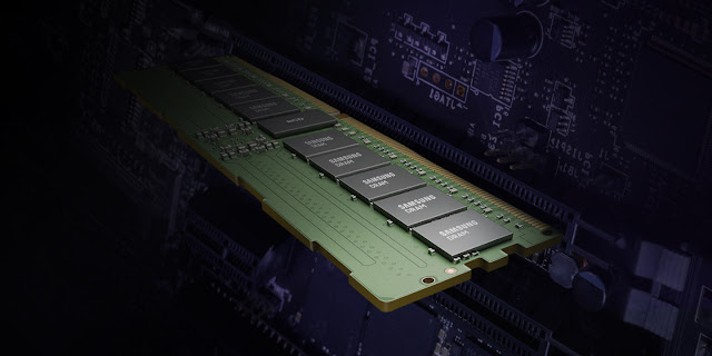
Qualcomm has certified Samsung’s LPDDR5X DRAM for use in Snapdragon processors
The EUV: breakthrough in memory technology
The most recent invention is ready for prime time, and it will significantly alter how electronics appear and work. Extreme Ultraviolet (EUV) lithography is the technique that makes it all possible. Higher performance in smaller sizes is becoming more important as memory-based technology advances in our data-driven environment. Samsung has pioneered EUV advanced processing to overcome DRAM scaling limits and to lead the next generation of memory manufacture.
Technology’s limits are being pushed
Samsung was the first in the industry to use manufacturing know-how to successfully apply EUV processing to DRAM manufacture, and it has been mass-producing specialised EUV-applied products. In EUV processes, Samsung has the upper hand. Because of its outstanding semiconductor manufacturing technology and knowledge, it was one of the first in the industry to effectively use EUV processing to DRAM manufacture. Samsung has already begun mass-producing select EUV-applicated items and is planning to expand its capacity in the near future.
Compact sizes are more powerful
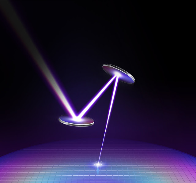
In comparison to the old 193nm wavelength, the EUV advanced processing technology uses a precise wavelength of 13.5nm. This permits the memory to store more capacity in the same amount of space and size, allowing it to satisfy future needs for high-capacity Non Volatile Memory.
Here’s the distinction. While DUV lithography utilises wavelengths of 193nm, EUV lithography employs wavelengths of 13.5nm, which is a significant improvement. As a result, finer circuitry may be drawn, allowing more data to be stored on the same surface area. More logical gates may be packed into a single chip when the circuitry is finer. As a result, those chips become more powerful and energy-efficient. When EUV is employed, the surface area of a chip is utilised considerably more efficiently, thus it’s no surprise that many in the industry are racing to develop the technology for their own fabrication lines.
Processing and productivity have improved
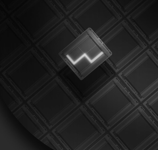
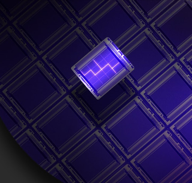
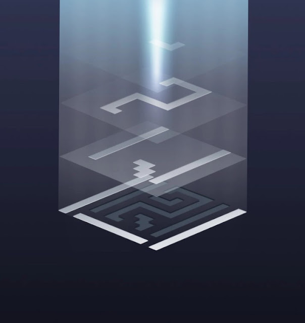
Single pattern, which uses modern processing technology, improves precision and reduces processing time as compared to multi-patterning, which uses a longer wavelength. When compared to earlier processing methods, this significantly improves wafer manufacturing efficiency.
 |
| Step-by-step Multi patterning |
 |
| Seamless-one-step Single patterning |
The memory market is quite competitive. However, there are no new steps that can be implemented quickly that will genuinely shake up the sector. As a result, it’s critical to get ready now for tomorrow. EUV lithography has a bright future for DRAM, but it’s Deep Ultraviolet (DUV) lithography that’s now in use. For current semiconductor generations, DUV works well.
You can rely on our quality
Samsung established confidence by preventing faults through manufacturing know-how based on the EUV logic process, and by progressively integrating EUV advanced technologies to increase quality early on.
For both quality and technology, the manufacture of EUV applied DRAM products has garnered international customer confidence and reputation. Look about you and you’ll almost certainly come across some form of technology that links to a larger network of devices. Indeed, the rise of IoT, AI, and 5G has necessitated modifications in the way DRAM is produced. Memory currently requires finer processing, and the EUV process’s highly fine ultraviolet light is exactly what the industry requires to develop DRAM solutions that will be extensively deployed in the future years.
A significant step forward in the future
Samsung changes the DRAM industry’s paradigm with industry-leading processing technologies that led to a new range of DRAM products. This never-say-die attitude cleared the way for the next generation of memory devices.
This is a trip, and we haven’t yet arrived at our destination. Samsung is aware of this and is working to correct any flaws now so that it can be ready for the future. The firm has a roadmap that outlines how it plans to expand the adoption of EUV-based DRAM products.
Samsung teases a Galaxy MWC 2022 event Expose about New Era of Mobile Devices
Samsung Electronics is once again changing the future of how we work and study in today’s quickly expanding world powered by mobile devices.
On February 27, come discover how Samsung is driving the connected experience at the Samsung Galaxy Mobile World Congress (MWC) Event 2022. Beginning at 7:00 p.m. CET, the event will be aired live on Samsung Newsroom and Samsung’s YouTube account.
With a showcase animation showing its variety of goods, including phones, foldable, smartwatches, tablets, and PCs, the business sent out its Galaxy MWC Event invitation for the “new age of connected devices.” Although the teaser is ambiguous, the firm has already released another MWC teaser that gives us a little more insight into what we may expect.
Samsung also does a proper job at this, as seen by the addition of One UI Watch to the Galaxy Watch 4, which allows for smooth interactions between the watch and Galaxy smartphones. Samsung has also launched new watch upgrades that improve the watch’s connection.
Note Series Power Meets S Series in the Galaxy S22 Ultra
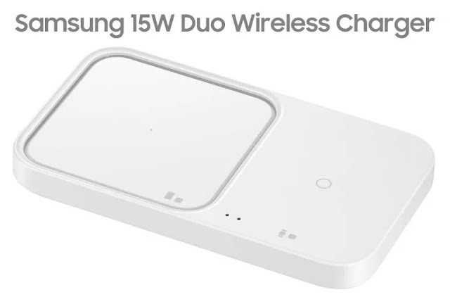
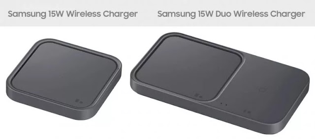
Samsung Galaxy S22 release two 15W Duo Wireless Charger
Samsung will unveil the Galaxy S22 smartphone lineup, as well as three Galaxy Tab S8 tablets, at Origen. Samsung will also unveil a number of new accessories at the same time. Consider a variety of smartphone covers and Book Cover Keyboard types to best protect the new gadgets. A number of additional chargers are also coming.
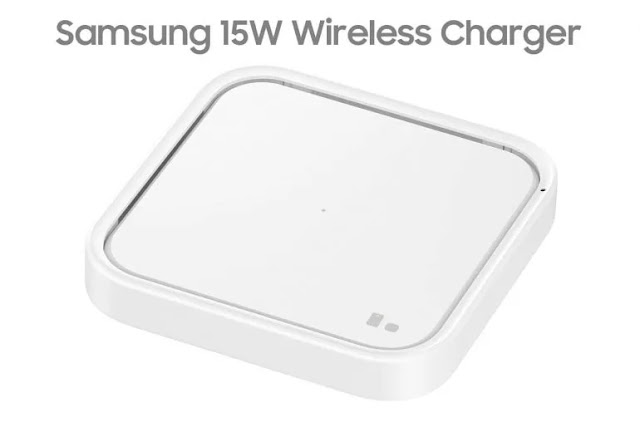
LetsGoDigital previously revealed that Samsung Netherlands’ website had a new 45 Watt USB-C adaptor displayed. Roland Quandt announced two new chargers via WinFuture today. A 15W Samsung Wireless Charger EP-P2400 and a Samsung Duo Wireless Charger EP-P5400 are involved.
Samsung Wireless Charger (15W)
Galaxy S22 devices are compatible with both wireless chargers. The adapters should be available within a few weeks of the release. The pricing has not yet been determined. There will be two versions available: one with and one without an adaptor.
The bases of the two wireless chargers are flat. With the possibility to flip out a section so that the smartphone may be used vertically if desired. According to WinFuture, the battery of the S22 can be completely charged in two hours using this 15W wireless charger, which also applies to the Galaxy S21 and Note 20 line of smartphones. The new wireless charger will be available in two colours: white and black. A 25W adaptor is compatible with the docking stations.
Smartphones with fast charging technology
Samsung isn’t instantly associated with the most advanced quick charging technology. Chinese smartphone manufacturers, in particular, provide much quicker charging technologies. Consider the Xiaomi 12 Pro, which comes with a 120W charger as standard, and the OnePlus 10 Pro, which has an 80W charger. Both gadgets were just introduced in China, but they won’t be available in Europe until later this quarter. Nonetheless, both wired and wireless charging is substantially faster on current models than on Samsung phones.
The major battery problem with the Note 7 cost Samsung a lot of money at the time. When it comes to maximum charge, it appears that the firm has subsequently opted not to go too quickly. This is also true of corporations like Apple and Google.
Quickly charging the battery entails concerns as well; for example, there have been several reports of exploding batteries with the OnePlus Nord 2 in India. Another drawback is that swiftly charged batteries do not keep their capacity for a long period — the differences might be seen after a year. Then your phone’s battery suddenly drains significantly faster. Overall, both tactics have their advantages and disadvantages.
Samsung Galaxy S22 Series Super Resolution camera Algorithm
The Samsung Galaxy S22 series of phones will be formally introduced on February 9, however, its official PPT has unexpectedly leaked ahead of time, nearly removing the mystery around this incoming new smartphone.
Although the 108MP main camera exists in the Galaxy S20 series, it previously only supported pixel digest mode and native mode for separate imaging and this is the first time two modes of the same main camera are used to enhance the final image. This time Samsung Galaxy S22 series, although the rear camera hardware changes little, with the support of the new algorithm, may also be worth the wait. This time, Samsung also added a new AI resolution function, which can invert AI to improve the clarity of 108MP mode, and combined with 12MP mode to improve the brightness performance of this model.
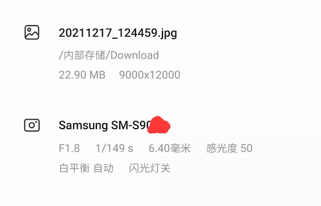
The upgraded mode’s 108-megapixel photo volume is higher, growing from 22.9MB to 32.27MB, and needs up to 2 seconds of background processing time while capturing images, according to Ice Universe. However, the final photographic details and post-production space are well worth the wait.
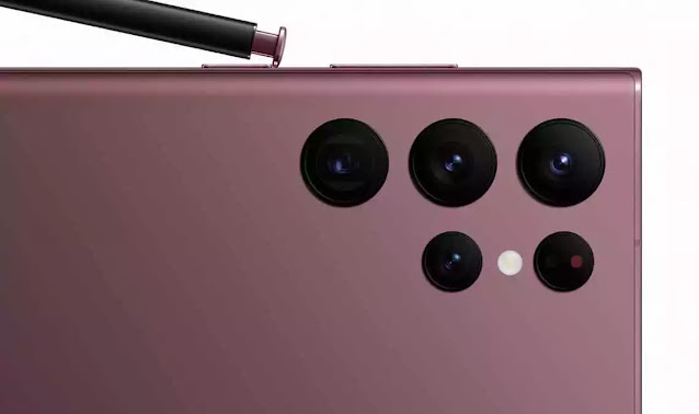
Camera Modules for Samsung Galaxy S22 Ultra
★12 MP F2.2 Ultra Wide (Dual PixelAF)
★OIS, wide 108 MP F1.8 (PD),
★Tele1 10 MP F2.4 (3x, Dual Pixel AF), OIS
★Tele2 10 MP F4.9 (10x, Dual Pixel AF) OIS
★F2.2 front 40 MP (PD)
Features of the Samsung Galaxy S22 Ultra Camera
★3x/10x Optical Zoom, 100X Space Zoom
★Scene analysis for more realistic, comprehensive videos
★For optimal detail and brightness, use the new Adaptive Pixel.
★Redesigned AI ISP for picture noise reduction
★Advanced VDIS for quicker phone and subject movement prediction
★For focussing on fast-moving objects, AI Scene Understanding is used.
★For a more detailed expression of the skin and brows, AI can be used.
★For better segmentation, use an AI Stereo Depth Map.
★Object Eraser for several viewing angles in a single picture Director’s View
★Optimization of performance for long-term use
Samsung has released a smart all-in-one fingerprint security IC for biometric payment cards
increased security capabilities offered by Samsung’s exclusive fingerprint authentication algorithm and anti-spoofing technology, the new security IC solution integrates a fingerprint sensor, Secure Element, and Secure Processor into one chip.
The new circuit Embedded Security is the industry’s first all-in-one security chip solution that reads biometric information via a fingerprint sensor, stores and authenticates, attracts encrypted data with a tamper-proof OS, and scans and processes data with a secure processor Three key functions integrated into a single chip, the S3B512C can help card manufacturers reduce the number of chips needed and optimize card design processes for biometric payment cards. integrated security, biometric payment cards will enable faster and more secure interactions during purchases. that eliminates the need for the ability to enter a PIN on a keypad and also prevents fraudulent transactions made with lost or stolen cards as it verifies identities using a unique and securely stored fingerprint.
Its solution’s encrypted fingerprint data is kept in a SE that has been certified by EMVCo and CC EAL 6+, two widely recognised security standards. The new IC has a patented fingerprint authentication algorithm and a Secure Processor that extracts and analyses the unique features of the fingerprint put on the sensor to safely and reliably authenticate the user’s identification. Furthermore, the chip’s anti-spoofing technology stops unauthorised users from bypassing the security system by using illegitimate means like fake fingerprints.
The Xclipse 920 GPU in the Samsung Exynos 2200 reveals benchmark results
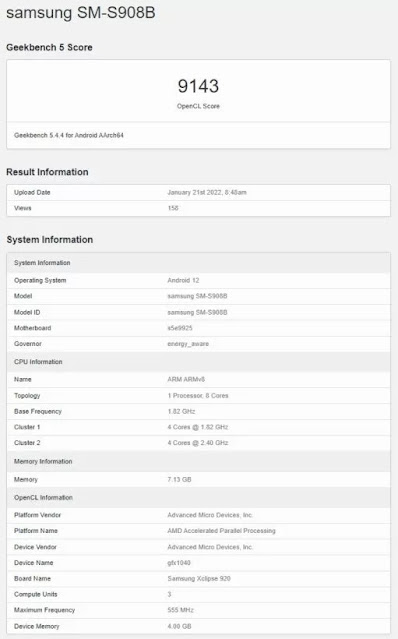
Samsung released the Exynos 2200 flagship chip this week, with a CPU architecture similar to the Snapdragon 8 Gen1 Dimensity 9000, but a GPU based on AMD RDNA2 to create the Xclipse 920, which supports advanced variable refresh rate, ray tracing, and other features, claiming to provide an unmatched gaming experience.
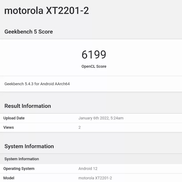
Additionally, Geekbench boasts 4GB of video memory (which should be shared by system RAM) and 384 stream processors. In a side-by-side comparison, the Snapdragon 8 Gen1 is around 6200 in the same test, the Snapdragon 888 is around 4835, and the Apple A15 Bionic is 14556. The Exynos 2200’s end performance is still quite promising, at least as far as these performances are concerned. Of course, in addition to card performance, final power consumption, temperature control, ion set optimization, etc. also need to practice for the final test.
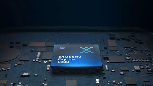
Samsung Exynos 2200 is one of the most recent Armv9 CPU cores to be released. One Arm Cortex-X2 core, three Cortex-A710 big cores for balanced performance and efficiency, and four tiny cores for energy efficiency make up the octa-core CPU’s tri-cluster architecture.


