Google launching Slovakia in News Showcase service
Samsung Galaxy A33 vs Galaxy A53 vs Galaxy A73 Specs Compare
The EUV: breakthrough in memory technology
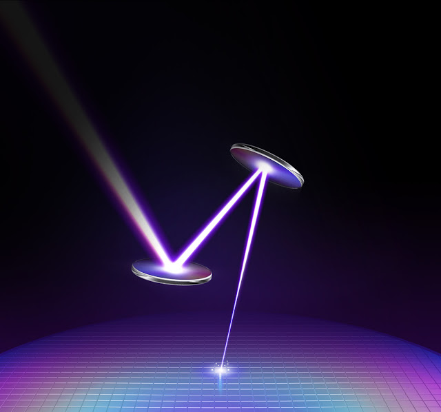
The most recent invention is ready for prime time, and it will significantly alter how electronics appear and work. Extreme Ultraviolet (EUV) lithography is the technique that makes it all possible. Higher performance in smaller sizes is becoming more important as memory-based technology advances in our data-driven environment. Samsung has pioneered EUV advanced processing to overcome DRAM scaling limits and to lead the next generation of memory manufacture.
Technology’s limits are being pushed
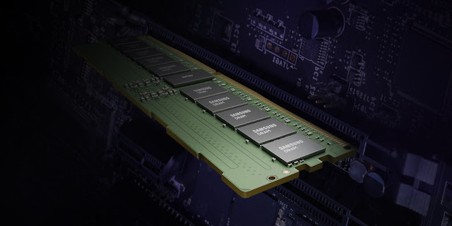
Samsung was the first in the industry to use manufacturing know-how to successfully apply EUV processing to DRAM manufacture, and it has been mass-producing specialised EUV-applied products. In EUV processes, Samsung has the upper hand. Because of its outstanding semiconductor manufacturing technology and knowledge, it was one of the first in the industry to effectively use EUV processing to DRAM manufacture. Samsung has already begun mass-producing select EUV-applicated items and is planning to expand its capacity in the near future.
Compact sizes are more powerful
In comparison to the old 193nm wavelength, the EUV advanced processing technology uses a precise wavelength of 13.5nm. This permits the memory to store more capacity in the same amount of space and size, allowing it to satisfy future needs for high-capacity Non Volatile Memory.
Here’s the distinction. While DUV lithography utilises wavelengths of 193nm, EUV lithography employs wavelengths of 13.5nm, which is a significant improvement. As a result, finer circuitry may be drawn, allowing more data to be stored on the same surface area. More logical gates may be packed into a single chip when the circuitry is finer. As a result, those chips become more powerful and energy-efficient. When EUV is employed, the surface area of a chip is utilised considerably more efficiently, thus it’s no surprise that many in the industry are racing to develop the technology for their own fabrication lines.
Processing and productivity have improved
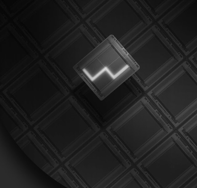
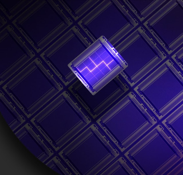
Single pattern, which uses modern processing technology, improves precision and reduces processing time as compared to multi-patterning, which uses a longer wavelength. When compared to earlier processing methods, this significantly improves wafer manufacturing efficiency.
 |
| Step-by-step Multi patterning |
 |
| Seamless-one-step Single patterning |
The memory market is quite competitive. However, there are no new steps that can be implemented quickly that will genuinely shake up the sector. As a result, it’s critical to get ready now for tomorrow. EUV lithography has a bright future for DRAM, but it’s Deep Ultraviolet (DUV) lithography that’s now in use. For current semiconductor generations, DUV works well.
You can rely on our quality
Samsung established confidence by preventing faults through manufacturing know-how based on the EUV logic process, and by progressively integrating EUV advanced technologies to increase quality early on.
For both quality and technology, the manufacture of EUV applied DRAM products has garnered international customer confidence and reputation. Look about you and you’ll almost certainly come across some form of technology that links to a larger network of devices. Indeed, the rise of IoT, AI, and 5G has necessitated modifications in the way DRAM is produced. Memory currently requires finer processing, and the EUV process’s highly fine ultraviolet light is exactly what the industry requires to develop DRAM solutions that will be extensively deployed in the future years.
A significant step forward in the future
Samsung changes the DRAM industry’s paradigm with industry-leading processing technologies that led to a new range of DRAM products. This never-say-die attitude cleared the way for the next generation of memory devices.
This is a trip, and we haven’t yet arrived at our destination. Samsung is aware of this and is working to correct any flaws now so that it can be ready for the future. The firm has a roadmap that outlines how it plans to expand the adoption of EUV-based DRAM products.
Sony Releases ‘LinkBuds’ a set of open design earbuds
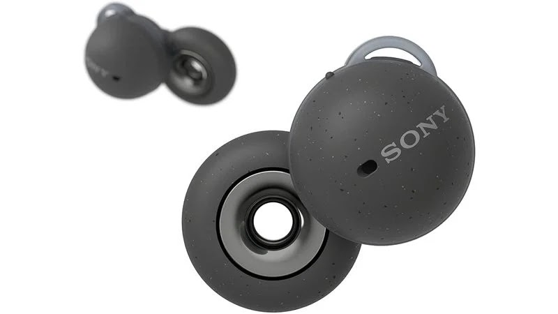
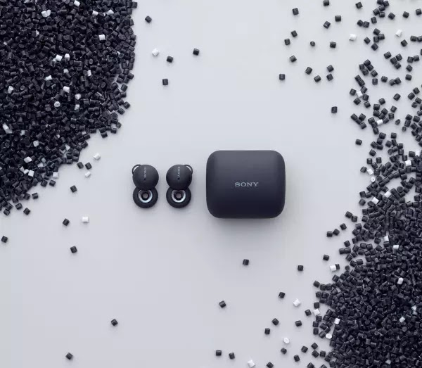
The Sony company’s latest truly wireless earbud device, the LinkBuds, was launched today. The LinkBuds offer a distinctive open-air design that sets them apart from conventional earbuds.
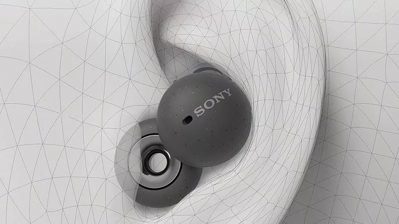
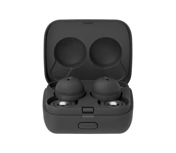
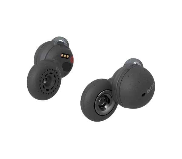
The LinkBuds have a doughnut-shaped earpiece that inserts in the ear and are available in black or white. The LinkBuds don’t come with any foam or silicone tips, like the AirPods 3, and the bare earpiece fits straight inside the ear.
The open ring driver in the LinkBuds allows users to listen to music while also hearing their surroundings, comparable to other headphone devices such as sound-equipped eyewear and bone conduction choices. Sony’s LinkBuds are perfect for scenarios when listeners need to be aware of their surroundings, such as walking, running, bicycling, or taking public transit, because they do not block ambient sound.
Sony characterises the earbuds as ultra-compact, light, and able to stay in the ears thanks to a secondary bulb with a little fin. They’re splash and perspiration resistant to IPX4, and an Adaptive Volume Control function adjusts the volume to match the sound in the surroundings. The LinkBuds have 5.5-hour battery life and come with a charging case that delivers a total of 17.5 hours of listening time.


