The lines between the metaverse and our everyday experience are becoming advanced as powerful graphics and display technologies progress. The improvement of memory solutions created specifically for visual items has made a significant portion of this crucial change conceivable.
Solution for High-bandwidth Graphics Memory
The complexity of replicating real-world items and situations in virtual spaces is one of the main obstacles to enhancing virtual reality. Massive amounts of memory and powerful computers are needed for this. The advantages of developing a more realistic metaverse, however, will be numerous and will spur innovation in a variety of industries, including real-life simulations of complex circumstances and more.
One of the most well-known virtual reality notions is the digital twin, and this is its fundamental tenet. A virtual depiction of an object or location is called a digital twin. A digital twin covers the lifespan of its source and is updated in real-time in line with the actual environment. It employs simulation, machine learning, and reasoning to aid in decision-making. Although up until recently, was not a practical idea owing to restrictions on data processing and transmission, high bandwidth technologies today make digital twins a viable option.
The gaming industry, like other digital advancements, depends on ongoing innovation to flourish, with fresh improvements in speed and performance propelling the sector ahead year after year. High-end AAA gaming graphics are getting more lifelike and engaging because of the development of technologies like Ray Tracing in 3D rendering, which tracks how light reflects in a particular scene.
‘GDDR6W’ Graphics Memory Development: Doubled Performance and Capacity
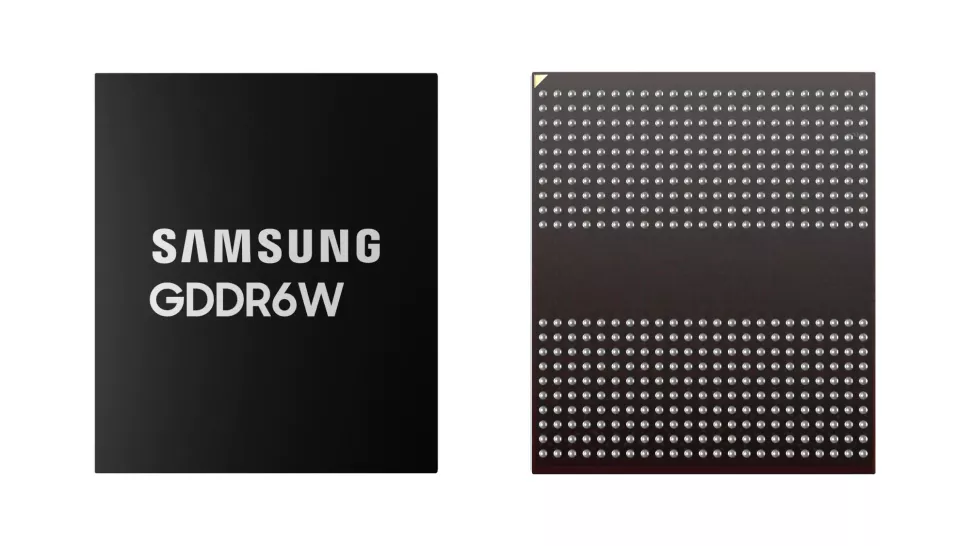
Memory solutions with high performance, large capacity, and high bandwidth are assisting in bringing the virtual world closer to reality. Samsung Electronics created GDDR6W (x64), the first next-generation graphics DRAM technology, to satisfy this expanding market need.
With the addition of Fan-Out Wafer-Level Packaging (FOWLP) technology, GDDR6W significantly boosts memory bandwidth and capacity over Samsung’s GDDR6 (x32) products.
GDDR6 has already experienced major advancements since its release. The fastest graphics DRAM on the market, 24Gbps GDDR6 memory, was created by Samsung in July. GDDR6W has the same size as GDDR6, but it has twice the bandwidth (performance) and capacity. With the usage of the FOWLP, new memory chips may simply be integrated into the same manufacturing procedures customers have used for GDDR6 thanks to the unchanged footprint.
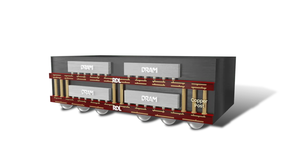
As additional chips are piled, a package’s size often grows. However, there are physical restrictions on a package’s maximum height. Additionally, even though stacking chips improve capacity, performance and heat dissipation suffer. We have integrated our FOWLP technology into GDDR6W to get around these trade-offs.
Instead of using a PCB, FOWLP technology places memory die directly on a silicon wafer. RDL (Re-distribution layer) technology is used in this process to enable considerably finer wiring patterns. Additionally, because there is no PCB involved, the package thickness is reduced, which enhances heat dissipation.
| GDDR6W | HBM2E | ||
| The number of System Level I/O | 512 | 4096 | |
| Pin Transmission Speed | 22Gbps | 3.2Gpbs | |
| System Level* Bandwidth | 1.4TB/s |
|
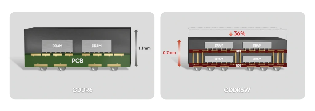
The FOWLP-based GDDR6W has a height of 0.7mm, which is 36% less than the previous package’s height of 1.1mm. The chip still delivers the same thermal characteristics and performance as the current GDDR6, while being multi-layered. However, unlike GDDR6, the FOWLP-based GDDR6W’s bandwidth may be doubled because of the increased I/O per single package.
At the system level, the recently created GDDR6W technology may enable bandwidth comparable to HBM. Based on 4K system-level I/O and a 3.2Gpbs transmission rate per pin, HBM2E has a system-level bandwidth of 1.6TB/s.
On the other hand, GDDR6W, which uses 512 system-level I/O and a transmission speed of 22 Gbps per pin, may generate a bandwidth of 1.4 TB/s. Additionally, as GDDR6W uses around 1/8 the amount of I/O compared to HBM2E, micro bumps are no longer required. Because there is no longer a requirement for an interposer layer, it is more affordable.
Samsung Electronics is moving forward with GDDR6W product standardisation. Additionally, it has stated that it would work with its GPU partners to broaden the use of GDDR6W to include new high-performance accelerators used for AI and HPC applications as well as compact form factor devices like laptops.
To get real-time news alerts join the Technewsrooms Telegram group. You can also follow us on Twitter and subscribe to our Google News feed for updates.



![[Unboxing]: Galaxy Z Flip4 Is Redesigned By Maison Margiela 12 [Unboxing] Galaxy Z Flip4 Is Redesigned By Maison Margiela](https://technewsrooms.com/wp-content/uploads/2022/12/Unboxing-Galaxy-Z-Flip4-Is-Redesigned-By-Maison-Margiela-96x96.webp)

