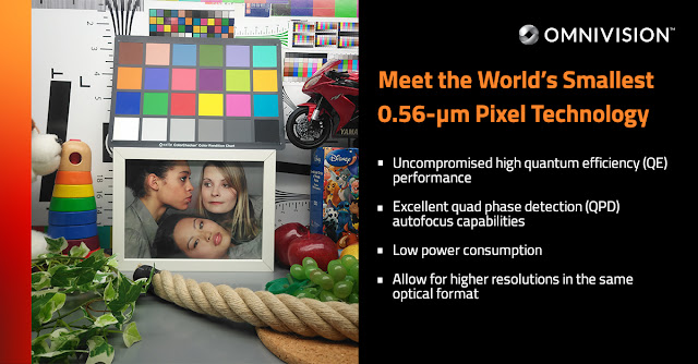
OmniVision proves that the wavelength of light has no bearing on pixel shrinkage; a revolutionary semiconductor device stacking method permits ultra-small 0.56 m pixels with good QE performance.
World’s Smallest 0.56μm Pixel Technology by OmniVision
The world’s smallest 0.56-m pixel with uncompromising high quantum efficiency (QE) performance, excellent quad phase detection (QPD) autofocus capabilities and low power consumption was announced today by OmniVision, a leading global developer of semiconductor solutions, including advanced digital imaging, analogue, and touch & display technology. The growing need for high-resolution and small-pixel pitch image sensors for multi-camera mobile devices will be met by this ultra-small pixel technology.
The R&D team at OmniVision has confirmed that pixel shrink is no longer restricted by the wavelength of light, with a pixel size lower than the wavelength of red light. A CMOS image sensor (CIS)-dedicated 28 nm process node and 22 nm logic process node at TSMC, as well as a novel pixel transistor layout and 24 shared pixel architecture, allow the 0.56 m pixel design.
OmniVision’s PureCel®Plus-S stacking technology is used to create the pixel, and deep photodiode technology is used to properly embed the photodiode further into the silicon. These creative technologies have enabled OmniVision to build the tiniest pixel, allowing for better resolutions in the same optical format, as well as more ISP capabilities, reduced power consumption, and faster image sensor processing.
“We are happy with the results of our close cooperation with OmniVision in delivering the world’s lowest 0.56-m pixel utilising our industry-leading CIS technology,” said Sajiv Dalal, TSMC North America’s Executive Vice President of Business Management. “TSMC works hard to enhance semiconductor manufacturing methods and services so that the most sophisticated, cutting-edge CIS designs may be realised.”
We look forward to working with OmniVision in the future to help them accomplish their high-performance, superior resolution, and low-power consumption goals, as well as accelerate innovation for their distinctive products.”
In Q2 2022, the first 0.56 m pixel part will be used in 200MP picture sensors for smartphones, with samples expected in Q3. In early 2023, consumers may expect to see new smartphones with the world’s tiniest pixel on the market.
To get real-time news alerts join the Technewsrooms Telegram group. You can also follow us on Twitter and subscribe to our Google News feed for updates.


