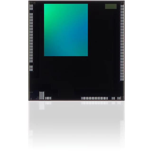
Japan’s Atsugi The IMX611 is a direct time-of-flight (dToF) SPAD depth sensor for smartphones that has the greatest photon detection efficiency in the market, according to a recent announcement by Sony Semiconductor Solutions Company (SSS).
The single-photon avalanche diode (SPAD) pixel structure of the IMX611 gives it the best photon detection efficiency in the market—28%. This enables a very accurate assessment of an object’s distance while lowering the system’s overall power consumption.
By the use of distance-based features and applications, this new sensor will open up new possibilities for smartphones.
| Model name | Sample shipment date (planned) | Sample price (including tax) |
|---|---|---|
| IMX611 1/8.1 type (2.2 mm diagonal) approx. 23,000 effective-pixel SPAD ToF depth sensor | March 2023 | 1,000 yen |
In a dToF sensor, SPAD pixels are commonly employed as a sort of detector to measure the duration of flight of light emitted from a source until it returns to the sensor after reflecting off an object.
It is possible to identify even extremely weak photons that have been generated from the light source and reflected off the object with the IMX611 because of its patented SPAD pixel structure, which has the best photon detection efficiency in the industry (28%). This makes it possible to estimate the distance between objects very precisely. Also, it implies that the sensor can provide accurate distance measurements even with a reduced laser light output, which contributes to a reduction in the overall power consumption of the smartphone system.
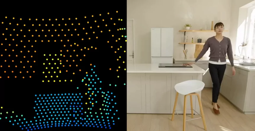
Its sensor’s ability to precisely gauge the distance to an item makes it possible to enhance focusing performance in dimly lit areas with limited vision, add a bokeh effect to the backdrop of the subject, and transition between wide-angle and telephoto lenses without missing a beat. The user experience with smartphone cameras will be enhanced by all of these features. Together with other similar features, this sensor offers 3D spatial identification, AR occlusion, motion recording, and gesture recognition. This sensor will help VR headsets and AR glasses, which are anticipated to see rising demand, become more useful as the metaverse spreads in the future.
 AR Occlusion
 AR Map
Main Features
The best photon detection efficiency in the market enables very precise distance measuring and minimal power usage
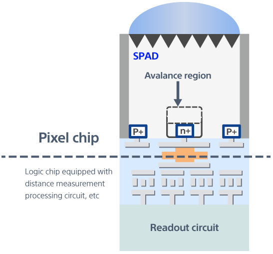
A Cu-Cu connection is employed in the stacked architecture of the IMX611 to achieve conduction for each pixel between the logic chip with a distance-measuring processing circuit and the back-illuminated SPAD pixel chip (top) (bottom). SSS has managed to reach a pixel size of 10 m square, which is fairly tiny for a SPAD, while still assuring a good aperture ratio by positioning the circuit under the pixel chip. The pixels have also undergone the following advancements thanks to SSS:
By employing a wavelength of 940 nm, which is frequently used in laser light sources for smartphones, these patented pixel architectures work together to give the industry’s greatest photon detection efficiency, at 28%. This allows for extremely precise detection and lowers the system’s total power usage.
The use of proprietary signal processing techniques streamlines system development
The RAW data obtained from the SPAD pixels is translated into distance information to be output by integrating a proprietary signal processing function onto the logic chip inside the sensor. By using this method, it is feasible to lighten the burden of post-processing and streamline system development as a whole.
| Model name | IMX611 | |
|---|---|---|
| Effective pixels | 140 x 170, 23,000 pixels | |
| Image size | Diagonal 2.2 mm (1/8.1-type) | |
| SPAD unit cell size | 10.08 x 10.08 µm | |
| Recommended light source wavelength | 940 nm | |
| Photon detection efficiency | 28% | |
| Power consumption at 8m*6 (long-distance mode) | 110mW (sensor) 160mW (system*7) | |
| Power consumption at 3m*6 (short-distance mode) | 40mW (sensor) 85mW (system*7) | |
| Distance precision*6 | Less than 0.1% error | |
| Distance signal processing | Included in the sensor’s logic chip | |
