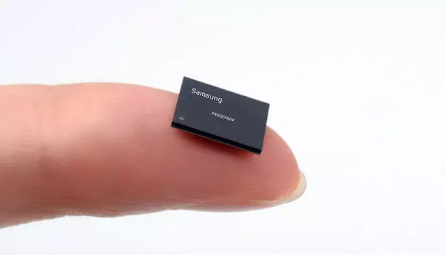
On January 11, 2022, Samsung will release its Exynos 2200 flagship chipset

Qualcomm unveiled the Snapdragon 8 Gen 1 SoC earlier this month, while MediaTek unveiled its flagship Dimensity 9000 processor. These chipsets will be seen in flagship phones next year, while some recently released phones will already be using the Snapdragon 8 Gen 1 SoC.

Samsung Exynos 2200

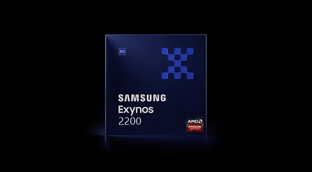
Now it appears that it is Samsung’s time, as the company stated today that the Exynos 2200, their next Exynos chip, will be unveiled around early January 2022. Samsung’s internal CPU for flagship phones, the Exynos 2200, will be unveiled on January 11, 2022. With the hashtag #PlaytimeIsOver, the firm previewed the new chipset’s performance. Unfortunately, the manufacturer hasn’t provided any specific information regarding the processor.

What we do know is that the company won’t be using a 4nm process like the Snapdragon 8 Gen 1, but it could have the same 5nm process seen in the Exynos 2100. This time around, the new Exynos 2200 will drive the graphics of the RDNA2 GPU. from AMD that you see on the PC and the console. help, it will come with awesome features like ray tracing and variable speed shading.

#PlaytimeIsOver. The gaming marketplace is about to get serious. Stay tuned for the next #Exynos with the new GPU born from RDNA 2. January 11, 2022. pic.twitter.com/0H2MeVUbeS

— Samsung Exynos (@SamsungExynos) December 30, 2021

With one CortexX2 processing core, three CortexA710 processor cores, plus four CortexA510 processor cores, the Exynos 2200 will become an octa-core chipset. It’s also likely to include a faster 5G modem, enhanced picture signal processing, and AI processing. In some areas, the Exynos 2200 will undoubtedly be found in Samsung’s upcoming flagships, such as the Galaxy S22, Galaxy S22 Plus, and Galaxy S22 Ultra. The Galaxy S22 will be available in the remainder of the world, including India and China, using Snapdragon 8 Gen 1 processors.
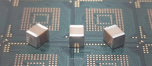
MLCC for 5G base stations has been developed by Samsung Electro-Mechanics.

On November 23, Samsung Electro-Mechanics announced the development of a high-capacity, high-voltage MLCC for 5G communications base stations. Samsung Electro-Mechanics’ new MLCC has a size of 3,225 (3.2mm wide, 2.5mm high), a high capacitance of 10uF (microfarad), and a high rated voltage of 100 V (higher voltage than the equipment can handle without being destroyed by the voltage) (volts).

Samsung ElectroMechanics' new MLCC

Samsung ElectroMechanics plans to ship this product to global telecommunications equipment partners starting next month. ※ Multilayer Ceramic Capacitor (MLCC), a major component of electronic devices that controls stable current flow in electronic circuits, it is essential for products such as smartphones, household appliances and cars. 5G communication can process large amounts of data at high speed using high-frequency bands, which requires many base stations due to the use of high frequencies. Compared with 4G LTE, 5G communication base stations have more transmitting antennas and rooms with higher power consumption and heat output. 

Therefore, MLCCs mounted on 5G communication base stations must be a large capacity to minimize component mounting area and provide stable power. In addition, high voltage products are required due to the characteristics of the base station which use high operating voltages to reduce power loss and the products must also be highly reliable to operate normally in the face of environmental changes such as temperature. and humidity. The MLCC developed by Samsung ElectroMechanics this time reached the high capacitance of 10uF to provide fast and stable power to high-performance semiconductors. In addition, it can replace two to three low-capacity MLCCs, thereby reducing the component mounting area. In addition, the rated voltage of 100V can be safely applied to 5G communication base stations, and the increased reliability allows the MLCC to operate normally against environmental changes such as external shock and vibration, temperature and humidity. In particular, the new product benefits from the best tensile strength in the industry with a guarantee of 3mm.

Samsung ElectroMechanics' new MLCC

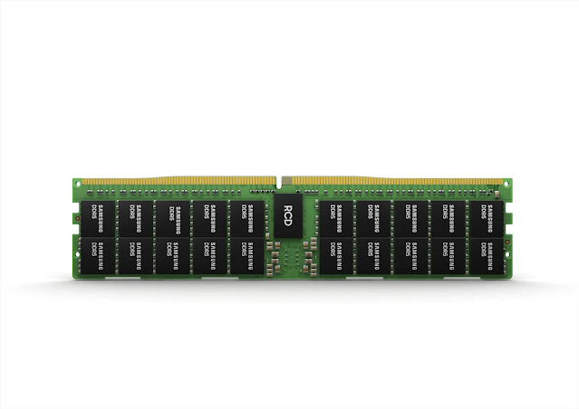
DDR6 / GDDR6+ memory solutions from Samsung will be 2x faster.

DDR6 memory is being developed by Samsung Semiconductor for next-generation computer products. Customers will have to wait at least a few years for the new standard, which will be twice as fast as the present DDR5 option. Samsung also mentioned the future of GDDR memory, which is critical for graphics cards, in addition to DDR6 memory, which will be utilised with CPUs.

Samsung Semiconductor

According to a recent article from ComputerBase, the corporation is still in the early phases of DDR6 research, but the standard might be finished in 2024 through continuing work with JEDEC members. JEDEC is an independent semiconductor standards body with over 300 members. 


In every way, DDR6 will be twice as fast as DDR5.

Once DDR6 memory is available, customers should experience data rates twice as fast as DDR5 solutions. Similar to how DDR5 doubled DDR4 data rates, the upcoming DDR6 standard is expected to do the same and thus achieve transfer rates of around 12,800 Mbps on JEDEC modules. That is about 17,000 Mbps overclocked.

Samsung Semiconductor

Additionally, DDR6 will have twice as many memory channels as DDR5, i.e. four 16-bit channels and 64 memory banks. As for LPDDR6 (Low Power DDR), Samsung doesn’t seem to plan to increase transfer speeds over LPDDR5, but the company is reportedly looking to achieve a 20% increase in power efficiency. 

GDDR6 will be replaced by GDDR6+ by Samsung.

While Samsung will likely release GDDR7 in the distant future, the company plans to offer a faster solution than GDDR6 as a bridge between the two generations first. Called GDDR6 +, the memory standard will be an improvement over GDDR6. GDDR6 + memory would reach speeds of up to 24 Gbps per pin, meaning GPUs with 256-bit buses could achieve a bandwidth of up to 768 Gbps. In turn, GPUs with a bus of 320 bits or more could exceed 1TB / s of bandwidth.

Samsung Semiconductor

As for what’s coming after GDDR7, it could be twice as fast as GDDR6 and a max throughput of 32Gbps per pin. However, there is no official roadmap for GDDR7, so the next GDDR6 + solution could take its place for a few years to come.


Samsung’s Cutting-Edge technology 2.5D Integration H-Cube Solution Announced.

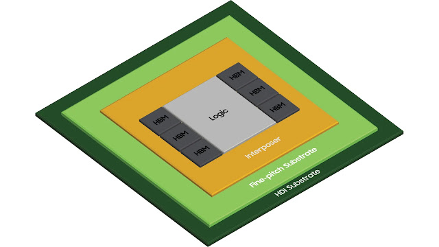
Samsung Electronics, a leading global in advanced semiconductor technology, today announced HybridSubstrate Cube (H-Cube) technology, it’s own latest 2.5D semiconductor packaging option special for HPC, AI products, networking, and data centre requirements which necessitate large-scale packaging technology.

2.5D Integration H-Cube

 “The H-Cube solution, developed in collaboration with Samsung ElectroMechanics (SEMCO) and Amkor Technology, is ideal for high-performance semiconductors requiring the integration of a significant number of silicon chips,” stated Moonsoo Kang, senior vice president and head of Samsung Electronics’ Foundry Business Model Team.” We will supply numerous packaging options to achieve a resolution in the issues our clients suffer by expanding and improving the foundry ecosystem.”

“In today’s environment, at which systems integration is becoming more important as well as surface supplies are becoming scarce, Samsung Foundry and Amkor Technology have successfully developed the H-Cube code to overcome this challenge,” stated “ JinYoung Kim, vice president of Amkor Technology’s Global RandD Center. “That invention lowers the entrance hurdle into the HPC/AI sector and illustrates a successful collaboration and partnership between both the foundry and the Companies outsource Semiconductor Running tests and Assembly (OSAT) firm.”

Structure and Functions of the H-Cube

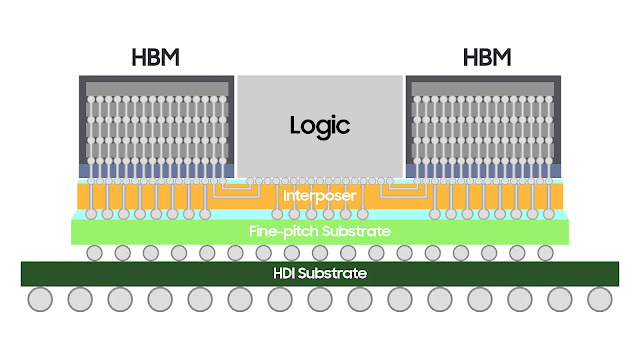
In a compact form factor, the 5D package allows users to install logic chips or high bandwidth memory (HBM) on top of a silicon supplements. Samsung’s H-Cube system involves a hybrid platform with a fine pitch platform capable of fine bump connections and a high density interconnection (HDI), allowing huge sizes to be implemented in a 2.5D packaging. Large-area packaging is becoming more significant when the quantity & size of chips put in a package grows or increases, as the consider in the HPC, AI, and network application market sectors have recently increased. It is necessary to have high-speed broadband communication. Fine pitch substrates are required for the attachment and connecting of silicon chips, including the interposer, but their costs rise significantly as the size grows.

2.5D Integration H-Cube
Concept of H-Cube Package Structure

If six or more HBMs are combined, the challenge of creating the huge substrate grows quickly, lowering efficiency. Samsung resolved the challenge by using a hybrid substrate structure that combines easy-to-process HDI substrates with a high-end fine-pitch platform over a large expanse. Due to a 35 percent reduction in solder ball pitch, that electrically links the chip and platform, the size of the fine pitched platform may be reduced, while an HDI substrate (PCB module) can be added beneath the fine pitch substrate for secure interaction with the board system. Furthermore, in order to increase the H-Cube solution’s dependability, Samsung’s unique power and signal integrity analysis technology has been used to deliver steady power while reducing signal loss or distortion while stacking numerous logical and HBM chips.

The world’s first LPDDR5X DRAM is developed by Samsung.

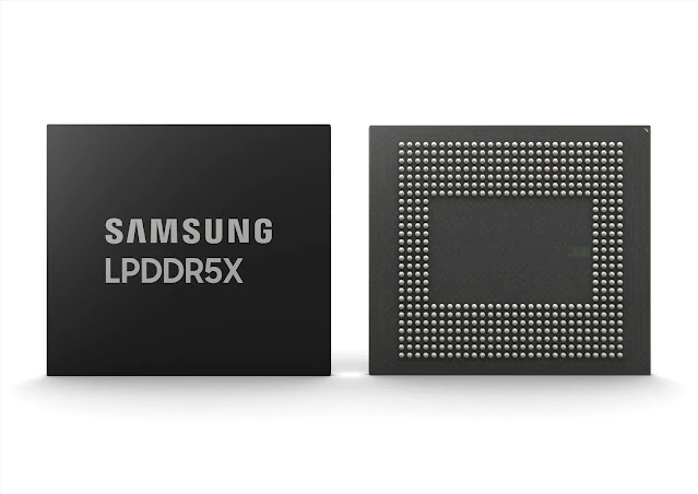
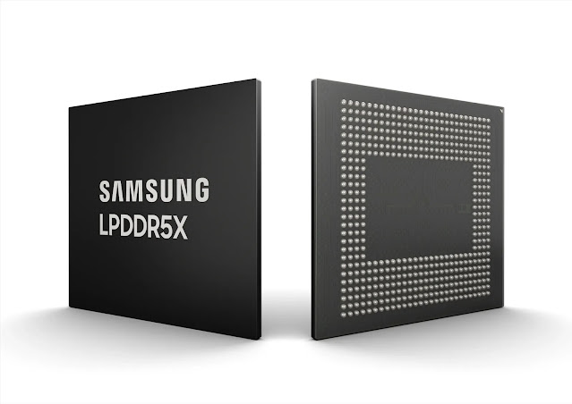
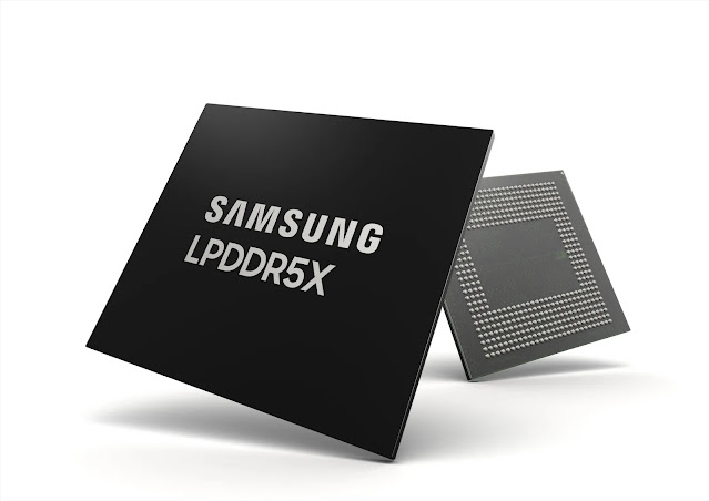
Samsung’s LPDDR5X DRAM offers over 1.3x higher processing rates while using over 20% less power than the prior LPDDR5 technology. Outside smartphones, the LPDDR5X solution will expand the usage of high-performance, low-power memory to AI and IoT technologies.

LPDDR5X DRAM

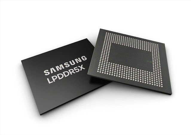
Samsung Electronics, a global leader in innovative memory technology, today announced the development of the industry’s first 14-nanometer (nm) based 16-gigabit (Gb) Low Power Double Data Rate 5X (LPDDR5X) DRAM, targeted at improving development in high-speed data development services such as 5G, AI, and the virtual world.

“Hyperconnected market areas such as AI, smart glasses (AR), and the metaverse, which rely on highly fast big data processing, have been quickly developing in recent times,” stated SangJoon Hwang, Senior Vice President and Head of Samsung Electronics’ DRAM Design Team. “In out LPDDR5X will expand the usage of high-performance, low-power memory beyond smartphones, bringing new possibilities to AI-based utilized to expand such as servers and even automobiles,” says the company.

LPDDR5X DRAM

Samsung’s LPDDR5X is a next-generation mobile DRAM that improves speed, capacity, and power efficiency for future 5G applications. Samsung introduced the industry’s first 8GB LPDDR5 DRAM in 2018, and the firm is now expanding beyond mobile markets with the introduction of the first 16GB LPDDR5X DRAM.

LPDDR5X DRAM

Its LPDDR5X DRAM will have processing capabilities of up to 8.5 gigabits per second (Gbps), which is more than 1.3 times better than the 6.4 Gbps of LPDDR5. This will require roughly 20% less power than LPDDR5 memory, thanks to the industry’s most sophisticated 14nm DRAM production technology. Also, the 16GB LPDDR5X chip will allow for up to 64 gigabytes (GB) of memory per memory packet.

Samsung will begin working with global chipset makers later this year to develop a more possible framework for the growing world of virtual reality, with its LPDDR5X acting as a crucial component of that groundwork.

LPDDR5X DRAM


With continuing advances in performance and power efficiency, the business will strive to expand its industry-leading mobile DRAM range, while also cementing its leading position with increased production flexibility.

A new DDR5 DRAM 14nm EUV technology is being mass produced by Samsung.

This industry-leading five-layer EUV process gives Samsung the highest bit density DRAM on the market, resulting in a 20 percent improvement in productivity over the latest DDR5 standard. Using Samsung’s 14nm DRAM, AI workloads and 5G workloads can be handled efficiently.

AVvXsEj7RDqHoWRk30UGa3Wk5oPmrlKTKsZpJy7W0Yj09sMa6hg1BdyI2Y1VOthc2Ld8kG9LlJjxu m51nooEdYy6GULcEae8gKupNP7eUd9pFkDzWBfdlpIdbyQcg8TwlhdMhM7ZlWqI3ywdDy1H3Rhxl g6rP3kwtPYcchEwAo0uDpZOs3M0trKWAeu7rNmA=w640 h452

The world’s leading memory company, Samsung Electronics, today announced the advent of its ultra-thin, nanoscale 14 nanometer (nm) high-speed DRAM, manufactured with EUV technology. The industry’s first EUV DRAM was delivered last March by Samsung, and Samsung has now increased layer counts to five so that its products are built with the most robust and advanced DRAM processes available today DDR5. Senior Vice President and Head of DRAM Products and Technologies at Samsung Electronics.

Today, Samsung is taking a new technological step forward with the multilayer UVV which has enabled extreme miniaturization at 14nm, a feat not possible with the conventional argon fluoride (ArF) process.  this advancement we will continue to provide more differentiated memory solutions by fully addressing the need for better, more capable cities in the data-driven world of 5G, artificial intelligence and metaverse. As DRAM continues to expand the 10nm range , EUV technology is becoming more and more important to improve the accuracy of models for higher performance and yields. 

AVvXsEgdoAlanT4xdKGBGr0IF78Gf9OyHmh4GRnw8I09hyLE5CCgpEqtLsq9bfJ8d22Uk3uY6sy8AXqoeDY eTeMTz4eCVAeVTkrlNm9LwMM3p8SKK5O a tzE1QzEWpwIfncYWGL4wLcxXVrEo9gYIuN051juImU7LpOflj YwlxmdbaKKta5gnXYvzxaicvg=w640 h452

With five EUV layers at its 14nm DRAM, Samsung has achieved the highest bit density while improving overall productivity wafers by about 20% The 14nm process can help reduce power consumption by up to 20% compared to the previous generation DRAM node.

AVvXsEhXWtdPUoZBkOpmCab9KRrWQhm4EVm9VGYMPvzWgSfIljB43L gB035xpg uVM3BqF C59PTVf0dC2v1WuJSuTayoUNam8Ch3RpWzq4HyokoUfygdg53zXEUmkklttO7sClVzwj2uJ1IWyqIDInCg7Y0o5VAnv8oYFr8cG5Uijy5QZyjYZr8Znz9gkL5w=w640 h452

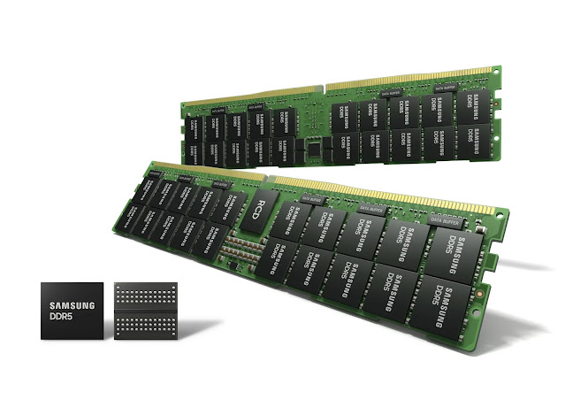
Taking advantage of the latest DDR5 standard, Samsung’s 14nm DRAM will help unlock unprecedented speeds of up to 7.2 gigabits per second (Gbps), more than double the DDR4 speed of up to 3 , 2 Gbit / s. Samsung plans to expand its 14nm DDR5 portfolio to support enterprise data center, supercomputer and server applications. Additionally, Samsung plans to increase the density of its DRAM chip from 14nm to 24GB to better meet the rapidly growing data demands of global computer systems.

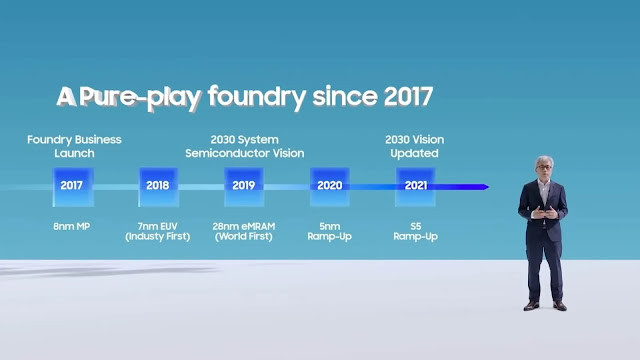
Samsung announces when it will begin manufacturing 2nm, 3nm, and 4nm chips.

 Samsung revealed its plans to manufacture semiconductor chips in mass quantities using 2nm, 3nm, and 4nm fabrication technologies. Samsung Foundry Forum 2021 brought this statement here. The world’s largest reminiscence chip logo unveiled that it’ll retain emigrate procedure technology for quicker and extra green chips, which might be in big demand, specifically because the COVID-19 pandemic.

AVvXsEjo4uPy58Ib7oMjgoPoKX9iwWZ4ffuCbYCO6trQHNe7KYpC98KsAV5MS0LvWYxId4CukQ Oiy6pDg3gUbgTNXgUZp8UXp 1BfXnWA4g9Lmq9l1HFn6GHbPeRHhpuPRLWM7NS5z9jQKjmVSbJrRp5i2XXrSws6Nv57i9hD QsOc0qiawc0Pgg9D5eb4ovw=w640 h320

South Korean firm Samsung Electronics announced that its 4nm technology has already been mass manufactured into chips. Additionally, Samsung Foundry found out that it will begin mass-producing semiconductor chips built on 3nm technology in the first half of 2022. Compared to the firm’s 5nm EUV process, its 3nm EUV process uses a GAA (Gate All Around) layout that can decrease bundle area by up to 35%, with better performance by 30%, as well as reduce power consumption by 50%.
AVvXsEjo9Z6t6y6WXppzRVtBLPmZmVqLXHyU5zlOogWkYjLSKsOAduO qZOPkfc5XVqBtCvI1Vqd9aqe5wq69RbSyQRwObLokRHlsb3xzqBuSnbM3cMuT79I53AdMfakVymRL1ZMPQHeMZN4428nQUO3RnUju1S DGcao0gf5mnqZ5hxuogK0dxAk3uxALimkg=w640 h360

The corporation additionally discovered that its 3nm technique’ yield is already coming near 4nm levels. Samsung’s second-technology 3nm procedure could be prepared for mass manufacturing someday in 2023. Samsung stated that it has currently introduced the 2nm technique node to its roadmap, and it’s miles presently below development. The corporation expects to begin the mass manufacturing of 2nm chips in 2025. This is the primary time Samsung is speaking approximately a 2nm technique, and it looks as if an optimized model of its 3nm technique node.

AVvXsEjWrE1fHmnjsjGHliuc2c zEpveczxt9c4gpJFSi rdTBQqkzMRRhsUDSrCQSVg93LkIdXasp7XOGV5MGJPV6cGaTgsdvY5 Q07a7fRTkcREc oHbO9rlpSbxdBvUqPxQuWs0ffX4n3NefkyQS7H5IQv6tM0rn8t4XcnqIc09 CYEXoX4KJqjXApYXytA=w640 h360

Samsung First Global Carbon Footprint Certification for Chips.

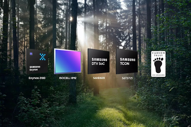
 Four high-performance, low-power chips have won the Carbon Trust label for measuring product carbon emissions, paving the way for reducing carbon emissions.

Carbon Footprint Certification 3

Samsung’s Green Manufacturing Efforts Continue to Expand Product Range Samsung Electronics, a global leader in advanced semiconductor technology, announced today that four LSI products have received the Carbon Trust Product Carbon Footprint Label, the first Samsung logic chip to do so. With the Semiconductor Industry’s first carbon certification for memory chips from the Carbon Trust in 2019, Samsung has expanded its ESG (Environment, Social and Governance) spectrum by globally recognizing its green logic chip.

Samsung also achieved the Carbon Trust’s first three industry standards for carbon, water and waste in June 2021. World advises companies on their capabilities in a sustainable manner. The Carbon Trust also measures and certifies the environmental impact of organizations, supply chains and products. Among the various certification categories of the Carbon Trust, Samsung Systems LSI products have received a CO2 label.

Carbon Footprint Certification 2

Samsung ElectroMechanics MLCC Development for ADAS

Samsung ElectroMechanics announced on the 12th that it has developed two types of automotive MLCCs, which are part of Advanced Driver Assistance Systems and # 40; ADAS ‘, a safe driving system essential for autonomous vehicles. (MLCC) is the main component of electronic devices that control the steady-state current in the circuit of electronic products and is required for smartphones, home appliances and cars.

imageView


recognize and assess possible situations during autonomous driving, including lane keep assist & # 40; LKAS & # 41; Surround View Monitor (SVM) and Intelligent Cruise Control (SCC). As vehicle functions improve, the number of semiconductor and high-performance components installed inside the vehicle is gradually increasing. In particular, the requirement for a self-propelled vehicle with a reliable power supply (source) and noise cancellation capability for various ICs to receive the signal quickly also requires small size and high MLCC capacity.

imageView%2B%25281%2529


Due to the lack of installation space with the increase in the number of components. size 0603 (width 0.6mm, length 0.3mm) and capacitance 100nF (nanofarad) and also high power product with 3216 (width 3.2mm, 1.6 mm) and a capacity of 47 μF (microfarads). ※ 1 μm (micro) = 1000 n (nano) MLCC 0603 delivers the same 100 nF (nanofarad) power as 1005, with a 64% reduction in surface area compared to size 1005 (1.0 mm width, length 0.5 mm). This product is installed on the signal head of the vehicle’s electronic control unit (ECU) to eliminate interference from ambient signals and accurately transmit the signal. In addition, the new product has twice the flexural strength of the standard product, which prevents the MLCC from being damaged by shocks and vibrations while driving, increasing product reliability. Specifically, the product complies with AECQ200, the automotive electronic component reliability test standard, so it can be used not only in ADAS but also in other applications such as body, chassis and infotainment system.

imageView%2B%25282%2529